Gallium nitride (GaN) is a material often used to build semiconductor power devices and light emitting diodes (LEDs). In the past, researchers have explored the possibility of realizing GaN p-channel transistors, which could aid the development of better performing computers.
Fabricating this type of transistor, however, has so far proved to be very challenging. A key reason for this is the low hole mobility of GaN, which essentially means that “holes” (i.e., missing electrons in the material) move too slowly through the semiconductor when an electric field is applied to it.
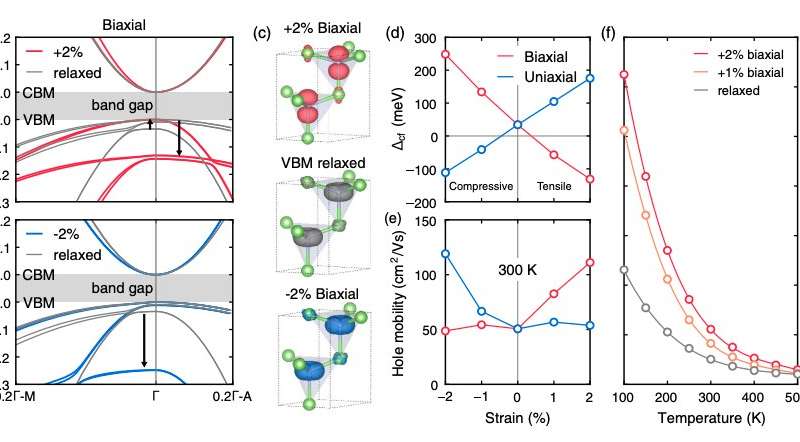
Researchers at Oxford University and Cornell University have recently carried out a study investigating the intrinsic phonon-limited mobility of electrons and holes in wurtzite GaN. Their observations, outlined in a paper published in Physical Review Letters, suggest that the hole mobility of GaN can be increased by reversing the sign of the crystal-field splitting, lifting the split-off hole states above light and heavy holes.
“We were working on developing computational tools for predicting the mobility of semiconducting materials starting from the fundamental equations of quantum mechanics and using high-performance computers,” Feliciano Giustino, one of the researchers who carried out the study, told Phys.org.
In physics, the mobility of charge carriers (e.g. electrons and holes), defines the speed at which these particles can move when a voltage difference is set up between the two ends of a semiconductor. Mobility is a key parameter that researchers need to consider when designing electronic and optoelectronic devices, including transistors used to fabricate microprocessors for smartphones.
“One of the key problems in high-power electronics and wireless communications is that the most widely used material, gallium nitride (GaN), has a very high electron mobility, but a very poor hole mobility,” Giustino explained. “As a consequence of this asymmetry, it is currently not possible to use GaN in the most fundamental circuit element of modern electronics, the complementary metal-oxide-semiconductor field-effect transistor (CMOS). In our research, we used supercomputers to design modified GaN materials with enhanced hole mobility.”
To carry out their research, Giustino and his colleagues used highly precise computer simulations of materials, in which each atom is described according to the fundamental laws of quantum mechanics. The theoretical formalism underlying their investigations relies on density-functional theory (DFT) and exploits general concepts of statistical mechanics, such as the Boltzmann equation. By combining these theories with massively parallel supercomputers, the researchers are able to predict the mobility of semiconductors with extremely high accuracy.
“In our approach we do not use any empirical parameters, we only specify the atomic species in the material (in this case gallium and nitrogen),” Giustino explained. “The methodology is implemented in our open-source software project EPW, which is available to everyone.”
The study carried out by Dr. Samuel Poncé, Prof. Debdeep Jena, and Prof. Giustino gathered several interesting observations. Firstly, the researchers discovered that by applying a tensile biaxial strain of 2 percent to GaN films that are approximately 10-30 nm in thickness, one can improve the semiconductor’s hole mobility by almost 250 percent.
“This enhancement is enough to enable the realization of GaN-based complementary metal-oxide-semiconductors (CMOSs), something that has remained elusive until now,” Giustino said. “At a more fundamental level, the effect that we discovered, which we named ‘reversal of crystal field splitting,’ is very intriguing because it results from a small re-ordering of the quantum states in GaN under strain.”
In the future, the observations gathered by this team of researchers could pave the way for the fabrication of GaN-based CMOS transistors. Prof. Giustino, who recently moved to the University of Texas at Austin, where he holds the Moncrief Chair of Quantum Materials Engineering, tells us that the next step will be to carry out a proof-of-concept experimental realization of the reversal effect observed in this recent work.
“Our collaborator and co-author Prof. Jena from Cornell University is a leader in the design and manufacturing of nitride materials and devices, and his group is attempting the fabrication of high-mobility GaN samples,” Giustino said.
