Humans have been studying electric charge for thousands of years, and the results have shaped modern civilization. Our daily lives depend on electric lighting, smartphones, cars, and computers, in ways that the first individuals to take note of a static shock or a bolt of lightning could never have imagined.
Now, physicists at Northeastern have discovered a new way to manipulate electric charge. And the changes to the future of our technology could be monumental.
“When such phenomena are discovered, imagination is the limit,” says Swastik Kar, an associate professor of physics. “It could change the way we can detect and communicate signals. It could change the way we can sense things and the storage of information, and possibilities that we may not have even thought of yet.”
The ability to move, manipulate, and store electrons is key to the vast majority of modern technology, whether we’re trying to harvest energy from the sun or play Plants vs. Zombies on our phone. In a paper published in Nanoscale, the researchers described a way to make electrons do something entirely new: Distribute themselves evenly into a stationary, crystalline pattern.
“I’m tempted to say it’s almost like a new phase of matter,” Kar says. “Because it’s just purely electronic.”
The phenomenon appeared while the researchers were running experiments with crystalline materials that are only a few atoms thick, known as 2-D materials. These materials are made up of a repeating pattern of atoms, like an endless checkerboard, and are so thin that the electrons in them can only move in two dimensions.
Stacking these ultra-thin materials can create unusual effects as the layers interact at a quantum level.
Kar and his colleagues were examining two such 2-D materials, bismuth selenide and a transition metal dichalcogenide, layered on top of each other like sheets of paper. That’s when things started to get weird.
Electrons should repel one another—they’re negatively charged, and move away from other negatively charged things. But that’s not what the electrons in these layers were doing. They were forming a stationary pattern.
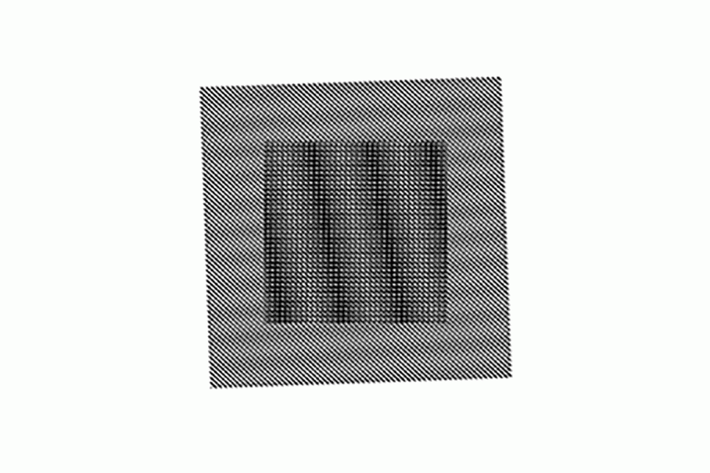
“At certain angles, these materials seem to form a way to share their electrons that ends up forming this geometrically periodic third lattice,” Kar says. “A perfectly repeatable array of pure electronic puddles that resides between the two layers.”Paragraph
At first, Kar assumed the result was a mistake. The crystalline structures of 2-D materials are too small to observe directly, so physicists use special microscopes that fire beams of electrons instead of light. As the electrons pass through the material, they interfere with each other and create a pattern. The specific pattern (and a bunch of math) can be used to recreate the shape of the 2-D material.