They call it “the shrink”—it’s the challenge of how to pack more circuits onto the microchips which power everything from our phones to our computers, even our coffee machines.
And pushing the boundaries of this technology is Dutch company ASML, which since its foundation in 1984 has quietly become a world leader in the semiconductor business.
“There is more power in your smartphone today than was used to put man on the moon,” says ASML’s chief operating officer Frederic Schneider-Maunoury, animatedly waving his mobile phone in the air.
When you open an app on your phone, the chain allowing you to book a flight, message a friend or check out who’s hot in your neighbourhood arcs all the way back most likely to ASML.
Headquartered in Veldhoven, near the Belgian border, it builds sophisticated lithography machines to enable the world’s top chip makers—Intel, Samsung and Apple supplier Taiwan Semiconductor Manufacturing (TSMC)—to produce the smallest, most powerful, most cost-effective microprocessors on the planet.
Its newest machines use highly-focused extreme ultra-violet (EUV) light to imprint designs on the chips, and are at the cutting-edge of what is scientifically and technologically possible in the art of miniaturisation.
‘Phones are not for calling’
Last year after two decades of research and development and billions of euros, ASML shipped its first 12 EUV machines to clients. Each costs about 120 million euros ($145 million).
This year it has projected sales of 20 machines—by 2020, it hopes to be selling 35 to 40 a year.
It is ironic that these machines, which produce chips of infinitesimally small dimensions, are the size of a bus. Three Boeing 747 aircraft are needed to transport one machine to a client.
Long seen as a bellwether of the tech industry, the company is listed on both the Amsterdam bourse, the AEX, and the Nasdaq in New York.
Last year it announced profits had almost doubled to 2.12 billion euros on record sales of 9.05 billion euros.
Only two other companies in the world—the Japanese giants Nikon and Canon—make lithography machines and neither has yet developed EUV technology.
“Our problem is not just to find the technologies, we than have to put it into the products in an economical way,” Schneider-Maunoury told AFP, in his office overlooking ASML’s sprawling site.
“Why buy a new phone? It’s not to make calls on. I buy a new phone precisely because it allows me to do things that the previous phone didn’t,” he said.
But this is a competitive market, and if the new phone “is going to cost me 10 times more, than I’m not going to buy it”.
A former vice-president at French rail giant Alstom, he joined ASML in 2010 and has become increasingly passionate about its innovative technology.
Accurate ‘to within an atom’
The EUV system works by projecting the light through a blueprint, ASML explains.
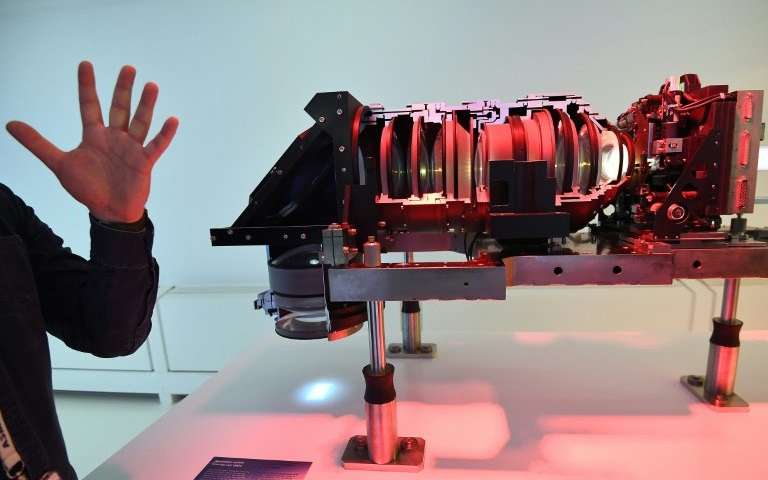
Using a series of complex optics, made by German company Zeiss, “the pattern is reduced and focused onto a thin slice of silicon coated with a light-sensitive chemical”.
“The light interacts with the chemical effectively printing the pattern onto the silicon or wafer. When the unwanted silicon is etched away a three-dimensional structure is created.” This is repeated dozens of times, layer upon layer, leaving a grid of hundreds of chips on one silicon wafer.
The light has to be focused in a vacuum to stop it being absorbed by air—a difficult technological feat—and the parameters are so small that the machine is working “to within the size of an atom”.
The tiniest speck of dust infiltrating the machine could ruin the design, leaving blank spaces on the chips.
ASML now employs about 20,000 people, mostly engineers and most in Veldhoven, but it also has sites in Asia and the United States.
And as it grows it is hiring. Some 3,000 new posts were added last year, with a similar number of new jobs expected this year.
