Organic-inorganic halide perovskite quantum dots (PQDs) form an attractive class of materials for optoelectronic applications. Their charge transport properties are, however, inferior compared to materials such as graphene. Conversely, graphene contains a charge generation efficiency that is too low for applications in optoelectronics. In a new report, Basudev Pradhan and a research team at the Nanoscience Technology Center, and the departments of Optics and Photonics, Materials Science Engineering, Physics and Chemistry at the University of Central Florida, U.S., Developed an ultrathin photon transistor and photonic synapses using graphene-PQD (graphene-perovskite quantum dot; G-PQD) superstructures. To prepare the superstructures they grew PQDs directly from a graphene lattice. Phototransistors made of G-QPDs exhibited excellent responsivity and specific detectivity. The light-assisted memory effects of the superstructures allowed photonic synaptic behavior for neuromorphic computing, which the team demonstrated through facial recognition applications with the assistance of machine learning. Pradhan et al. expect the G-PQD superstructure to bolster new directions to develop highly effective optoelectronic devices.
Graphene has emerged as a dream material for electronics and optoelectronics due to its broad spectral bandwidth, excellent carrier transport properties with high mobility, exceptional stability and outstanding flexibility. Materials scientists have developed many composites and devices for applications in energy harvesting, storage, photodetectors and transistors. However, a single layer of graphene can only absorb 2.3 percent of incident visible light, critically impeding their use in optoelectronic and photonic devices. In contrast, organic-inorganic PQDs have risen as attractive materials for applications in optoelectronics due to their unique characteristics, although their charge transport remains inferior compared to graphene.
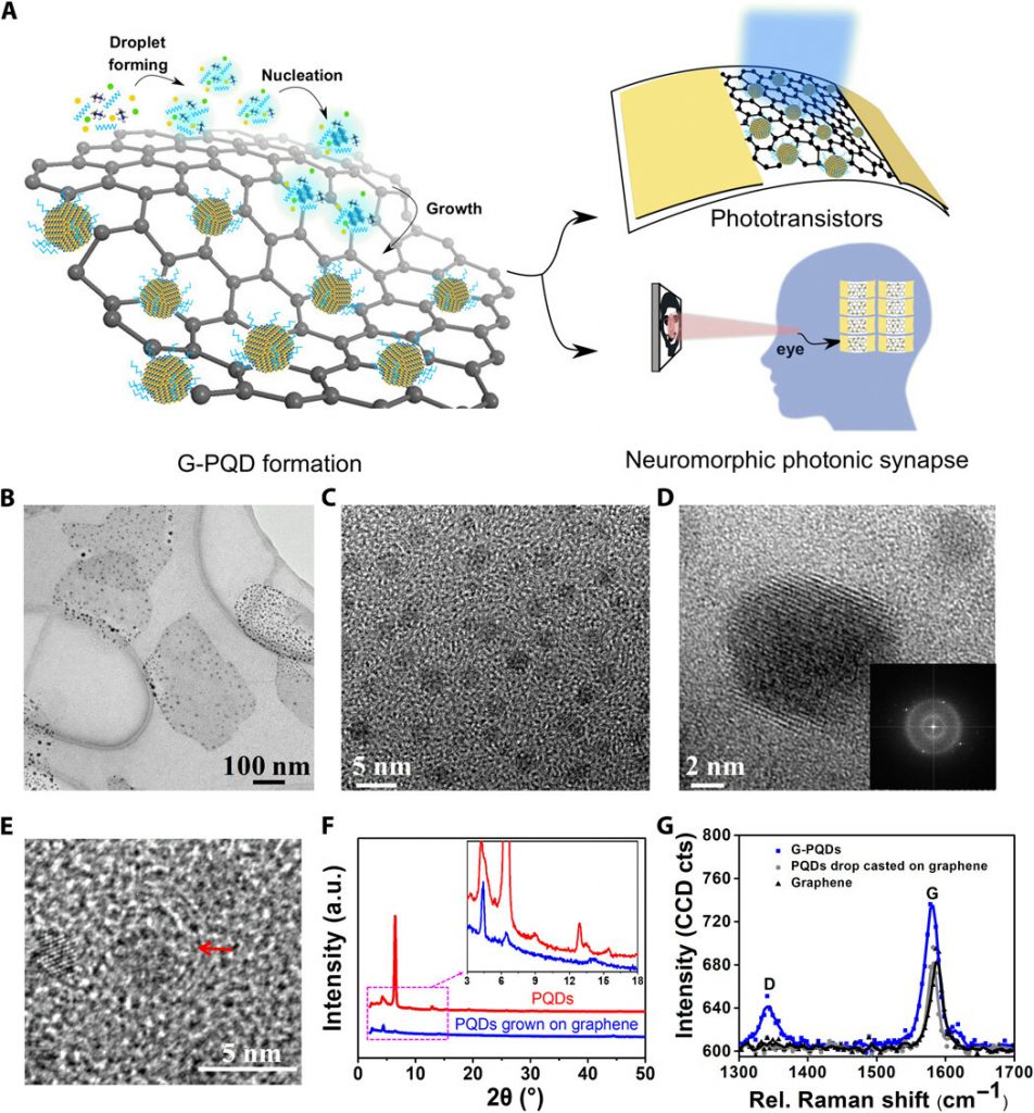
Growing PQDs from a graphene lattice
Pradhan et al. explored the strong photogeneration efficiency of methylammonium lead bromide PQDs in this work by growing PQDs from the lattice of single-layer graphene using a defect-mediated process. Since PQDs can absorb light and generate charge carriers, the rationale helped design the hybrid superstructures. The team implemented the thin superstructures in a phototransistor geometry to produce a photoresponsivity of 1.4 × 10⁸ AW-1 and a specific detectivity of 4.72 x 10¹⁵ Jones at 430 nm; which was by far the best responsivity and detectivity recorded across similar devices to date.
The work is highly promising to develop extremely efficient optoelectronic materials for high-speed communications, sensing, ultra-sensitivity cameras, high-resolution imaging and displays. The behavior of graphene-PQD (G-PQD) superstructures in the form of a photonic synapse is also critical for pattern recognition. The results support the development of a hardware unit for neuromorphic architecture that mimics the human brain—for a range of exciting applications. Pradhan et al. used ligand-assisted reprecipitation (LARP) to produce PQDs with a very high photoluminescence quantum yield, and controlled the size and morphology of the PQD products. The team initiated growth of PQDs directly on the active sites of the graphene monolayers to form the superstructures. During the process, they added an antisolvent toluene onto a graphene layer wetted with perovskite precursors to initiate seeding, and formed perovskite embryos on the graphene sheet required for PQD crystal formation.
The team analyzed the newly synthesized hybrid material (graphene PQDs) using transmission electron microscopy (TEM) to verify binding between the PQDs and graphene layers. They noted the presence of two different G-PQDs that absorbed visible wavelength at 434 nm and 451 nm, indicating their potential to form high-performing phototransistors detecting at blue illumination. Pradhan et al. tested the photophysical properties of the material relative to the excited-state dynamics of the G-PQD superstructure using time-correlated single photon counting (TCSPC) and observed an average fluorescence decay time of 749 ns. The superstructure showed enhanced sensitivity and an enhanced photocurrent compared to previously reported photoresistors. The device could also act as a light-activated switch under white light illumination and the photocurrent rose quickly within a response time of 0.45 seconds after turning the light on. Longer response times resulted due to more complex factors.
Since traditional von Neumann architecture or Princeton architecture; a computer architecture developed by mathematician and physicist John von Neumann is both time and power consuming for data transport at present. The existing limits of performance and scalability between the memory and processor are popularly referred to as the von Neumann bottleneck. The device had caused major drawbacks in data-centric applications of real-time image recognition, data classification and natural language processing. Neuromorphic computing is therefore an emerging—superior platform that can outperform the von Neumann architecture. In the setup, the synapse can typically act as a channel of communication between two neurons.
In this instance, the G-PQD superstructure acted as an artificial photonic synapse; where the pre-synaptic signal was based on the external light stimuli in the form of optical pulses and the post-synaptic signal was the current obtained across the G-PQD channel to keep the drain source and gate voltage fixed. The embedded optical information, detection processing and retention capabilities of the G-PQD synaptic devices formed a potential candidate for human visual memory in fields of pattern recognition. Pradhan et al. constructed a spiking neural network to perform unsupervised machine learning and face recognition using Python. The team used four portraits of people to train the neural network and showed that an increased use of output neurons alongside longer training time could achieve higher rates of facial recognition.
In this way, Basudev Pradhan and colleagues developed extremely thin superstructures based on hybrid materials of PQDs grown from a graphene lattice using a defect-mediated crystal growth technique. They obtained highly enhanced charge transfer due to the combined π-electron clouds of PQDs and graphene. The resulting devices exhibited high performances for phototransistors and photonic synapses, which the team further validated using simulations. The team intend to extend their approach to other 2-D materials including transition metal dichalcogenides and other heterostructures. The work will open the door to a new class of high-performance superstructure materials suited for multiple electronic and optoelectronic applications, beneficial for facial recognition and neuromorphic computing.