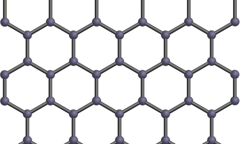
Physicists from the University of Sheffield have discovered that when two atomically thin graphene-like materials are placed on top of each other their properties change, and a material with novel hybrid properties emerges, paving the way for design of new materials and nano-devices.
This happens without physically mixing the two atomic layers, nor through a chemical reaction, but by attaching the layers to each other via a weak so called van der Waals interaction—similar to how a sticky tape attaches to a flat surface.
In the ground-breaking study published in Nature, scientists have also found that the properties of the new hybrid material can be precisely controlled by twisting the two stacked atomic layers, opening the way for the use of this unique degree of freedom for the nano-scale control of composite materials and nano-devices in future technologies.
The idea to stack layers of different materials to make so-called heterostructures goes back to the 1960s, when semiconductor gallium arsenide was researched for making miniature lasers—which are now widely used.
Today, heterostructures are common and are used very broadly in semiconductor industry as a tool to design and control electronic and optical properties in devices.
More recently in the era of atomically thin two-dimensional (2-D) crystals, such as graphene, new types of heterostructures have emerged, where atomically thin layers are held together by relatively weak van der Waals forces.
The new structures nicknamed ‘van der Waals heterostructures’ open a huge potential to create numerous ‘meta’-materials and novel devices by stacking together any number of atomically thin layers. Hundreds of combinations become possible otherwise inaccessible in traditional three-dimensional materials, potentially giving access to new unexplored optoelectronic device functionality or unusual material properties.
In the study researchers used van der Waals heterostructures made out of so-called transition metal dichalcogenides (TMDs), a broad family of layered materials. In their three-dimensional bulk form they are somewhat similar to graphite—the material used in pencil leads—from where graphene was extracted as a single 2-D atomic layer of carbon.
The researchers found that when two atomically thin semiconducting TMDs are combined in a single structure their properties hybridise.
Professor Alexander Tartakovskii, from the Department of Physics and Astronomy at the University of Sheffield, said: “The materials influence each other and change each other’s properties, and have to be considered as a whole new ‘meta’-material with unique properties—so one plus one doesn’t make two.
“We also find that the degree of such hybridisation is strongly dependent on the twist between the individual atomic lattices of each layer.
“We find that when twisting the layers, the new supra-atomic periodicity arises in the heterostructure—called a moiré superlattice.
“The moiré superlattice, with the period dependent on the twist angle governs how the properties of the two semiconductors hybridise.”
In other studies, similar effects have been discovered and studied mostly in graphene, the ‘founding’ member of the 2-D materials family. The latest study shows that other materials, in particular semiconductors such as TMDs, show strong hybridisation, that in addition can be controlled by the twist angle.
Scientists believe the study shows huge potential for the creation of new types of materials and devices.
Professor Tartakovskii added: “The more complex picture of interaction between atomically thin materials within van der Waals heterostructures emerges. This is exciting, as it gives the opportunity to access an even broader range of material properties such as unusual and twist-tunable electrical conductivity and optical response, magnetism etc. This could and will be employed as new degrees of freedom when designing new 2-D-based devices.”
Researchers would like to do further studies to explore more material combinations to see what the capabilities of the new method are.
Read more at: https://phys.org/news/2019-03-equal-graphene-like-d-materials.html#jCp
